Author: Nuha Akhtar
Mentors: Mohammad Mirhosseini, Hao Tian
Editor: Stephanie Chen
Abstract
Surface acoustic waves (SAWs) have become the ideal candidate for studying quantum behavior of macroscopic objects with the capability to be confined near the surface in compact resonators, excited and detected coherently through microwave electronics, and have its properties engineered based on the material of interest. Using piezoelectric materials, which have a unique property of electromechanical coupling, acoustic devices can be used in the quantum regime. Since functionality of a piezoelectric crystal is based on its physical parameters, this property-dependent performance acts as motivation in the search to find materials that will accomplish the task of sensing and actuating SAWs. Barium titanate (BTO) has become the piezoelectric crystal of interest due to its many excellent physical properties. Motivated by the limited amount of thin-film nanofabrication and analysis of material properties reported, a parameter space that maximizes the effect of BTO’s piezoelectric response was established through finite element analysis and material characterization. In the future, this information will allow for the fabrication of a successful SAW device that can be used to characterize BTO for a variety of quantum applications at the cryogenic level.
Introduction
Over the past two decades, there has been an increase in efforts toward the research and development of quantum systems. The application of quantum mechanics to develop a wide variety of quantum technologies has led to a new field of “quantum engineering”. In the field of quantum acoustics, surface acoustic waves (SAWs) have recently been used to develop new quantum technology. SAWs are sound waves that travel parallel to the surface of a material, with their displacement amplitude decaying quickly into the material. The quick decay into the material means the energy carried by SAWs is confined near the surface. Currently, SAW devices are routinely scaled down and integrated into compact circuits and sensors. They can quickly convert detected information into an electrical signal output, with real-time information detection characteristics. Due to the fact that “(1) SAWs are confined close to the surface, (2) they can be coherently excited and detected with microwave electronics, (3) stored in compact high-quality resonators or guided in acoustic waveguides over millimeter distances, and (4) their properties can be engineered by choice of material and heterostructure”, SAW devices are now seen as an ideal candidate for studying quantum behavior of macroscopic objects [1].
For an acoustic device to be used in the quantum regime, there needs to be a way to convert between its mechanical and electrical components. With transduction, the process of converting quantum signals from one form of energy to another is possible. To accomplish transduction using SAW devices, a piezoelectric material, which has the unique property of electromechanical coupling, is needed. The specifications necessary for a piezoelectric crystal to function are based on the material’s physical parameters, such as grain size and piezoelectric coefficient. The property-dependent performance of piezoelectrics acts as motivation in the search to find materials that will accomplish the task of sensing and actuating SAWs when an electrical voltage is applied.
Currently, piezoelectric materials, such as lithium niobate and aluminum nitride, have been used for quantum applications and information on their material properties is relatively established. In comparison, barium titanate (BTO) is a more novel material. BTO has a very high piezoelectric coefficient, which quantifies the volume change of a piezoelectric material subject to an electric field or the polarization caused by the application of stress. In fact, with a piezoelectric coefficient almost 6.5 times larger than lithium niobate, BTO is very appealing for acousto-optic and electro-optic applications, both of which are nonlinear processes where the change of the output is not proportional to the change of the input.
While there has been some recent electro-optical work done with BTO, there is little information about the thin-film piezoelectric properties of BTO. This study focused on the properties of thin-film BTO with an eventual end goal of studying the behavior of thin-film BTO at low temperatures. Through simulation, an optimized parameter space for a SAW device was created, enabling new device designs that will be used in the future to fabricate new optimized devices compatible with current BTO sample parameters. The simulation revealed that the current SAW devices being used had a suboptimal design. In addition, because BTO is also a ferroelectric, the electric domains in a BTO can be aligned with the application of a strong external electric field. This process of manipulating the domains of the crystal is called poling, a key feature of the material as it is both a piezoelectric and ferroelectric. Piezo-force microscopy (PFM) was studied to understand this process of poling and measuring BTO, confirming that BTO is capable of being poled and that PFM is a good tool for studying degrees of poling.
Methods
Simulation: Acoustic Modes
In order to characterize BTO via a SAW device, the first round of simulations were focused on studying SAWs and creating numerical designs of interdigital transducer (IDT) electrodes to find the optimal geometry to excite these SAW modes.
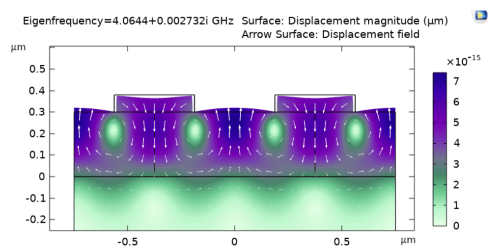
Because the goal is to use SAWs in a crystal, the correct acoustic mode must be used. This is the frequency at which a SAW is generated and propagated as a standing wave within the crystal. There are a variety of acoustic modes in the SAW family; this study focuses on Rayleigh and Sezawa modes. Rayleigh is considered a “first order” acoustic mode while Sezawa is the “second order”, or higher frequency, acoustic mode. The main difference between these modes is that the Sezawa mode has a primarily lateral component of displacement compared to the Rayleigh mode, as seen in Figures 1 and 2, which show plots of the magnitude of surface displacement for a Rayleigh and Sezawa acoustic mode.
Using a multiphysics simulation software, a 2D model of the SAW device was created, where many of the physical parameters of the device could be manipulated. This software allowed for a large range of frequencies to be applied to the simulated model and filter out results that did not create some type of excitation. With the filtered list of results, the plots produced in Figures 1 and 2 served as visual confirmation of an excited acoustic mode based on the symmetrical nature of displacement across the sample of three different thicknesses of BTO.

These eigenfrequencies then allowed for the coupling efficiency, kt , to be calculated. This efficiency is the fraction of electric energy that can be converted into mechanical energy and vice versa. Coupling efficiency is an important factor for this device, and one that would ideally be optimized to have higher values. By plotting the three BTO sample thicknesses versus varying IDT width, we were able to find and establish an optimized sample thickness with the highest coupling coefficient based on both Sezawa and Rayleigh acoustic modes.
Simulation: SAW Device Optimization
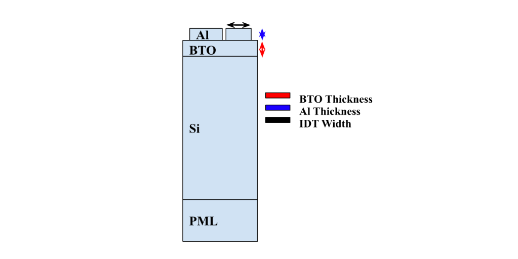
With the acoustic modes identified, the second round of simulations focused on manipulating a variety of parameters, which revealed that the three main variables that had the most impact on performance were BTO thickness, aluminum thickness, and the width of IDT. These parts of the device can be seen in the labeled side profile of a SAW device in Figure 3. A top view of the SAW device can be seen in Figure 4, including a close up image of the electrode fingers.

The electrodes allow for electro-acoustic coupling by converting microwave electric signals to SAW by generating periodically distributed mechanical forces via the piezoelectric effect. A flow of how the microwave signal travels through the device is shown in Figure 5. With the input terminal of the IDT connected to an alternating current (AC), a polarity of the interdigitated electrodes, alternated with the AC signal, forms as a result. This in turn generates alternating positive and negative electric fields between the fingers of the IDTs. Since we know that BTO is a piezoelectric and ferroelectric material, these alternating regions cause the domains of the material to either point towards or away the IDT, which induces mechanical strains; i.e., local tension and compression produced between the fingers of the electrodes.

The identified variables were then used in a third round of simulation to maximize the mechanical Q factor of the mode. The Q factor is a parameter that essentially describes the quality of resonance achieved by the device. A higher Q factor means stronger resonance with little dampening, also known as loss. Finding the Q factor was done by analyzing admittance, the ease with which an AC current flows through a system, and looking for well defined peaks and dips in the plots which would indicate a strong resonance.
In addition, the scattering parameter S11, which measures input voltage reflection, was used. Ideally at resonance frequency a small S11 reflection is desired, which indicates that at that frequency the majority of the energy is dissipated as acoustic energy.
Simulation: SAW Device Measurements
In order to measure the response of the current SAW devices, simulations were done to get a reference for the type of frequencies that should be expected experimentally. These frequencies would allow us to pole BTO and measure the response of the device as a function of IDT design. As IDT design was known to be suboptimal, a new method was needed to simplify the process of poling BTO and verifying if it had been poled successfully. Using PFM, it became possible to study the process of poling materials and measuring its response.
Piezo Force Microscopy
PFM is a type of high-resolution scanning probe microscopy that allows for characterization and manipulation of piezoelectric materials as well as obtaining nanoscale topography by using a physical probe that scans the samples surfaces. PFM measurements use the PFM amplitude signal, which provides information on the strength of the signal and thus the material’s piezoelectric tensor, as well as the PFM phase signal, which describes the direction of polarization.
Atomic Force Microscopy
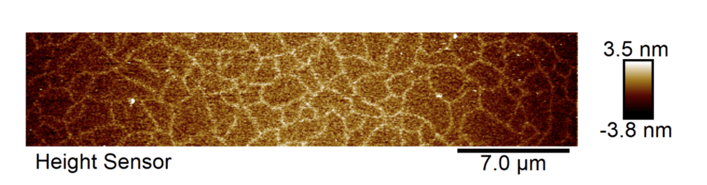
Atomic force microscopy (AFM) allowed for detailed images of the current SAW device. Figure 6 is a 3D image of the SAW device’s aluminum IDT using the AFM’s height sensor. In addition, detailed pictures of the BTO surface were also taken. Figure 7 is a 2D image of the BTO surface that highlights the varying grain sizes and boundaries.

Results
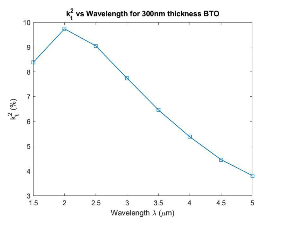
A 300 nm thick BTO sample with a Sezawa mode produced the highest value in simulation at approximately 9.7% coupling efficiency, as seen below in Figure 8. Alongside the optimized parameter space, simulations revealed that higher modes, such as the Sezawa mode, were more difficult to contain within the SAW device. Compared to the coupling efficiency of the Sezawa mode, the Rayleigh mode only had a coupling efficiency of approximately 5%, as seen in Figure 9. Even with this decrease in efficiency, parameter manipulations were based on the Rayleigh mode, in exchange for easier SAW containment.
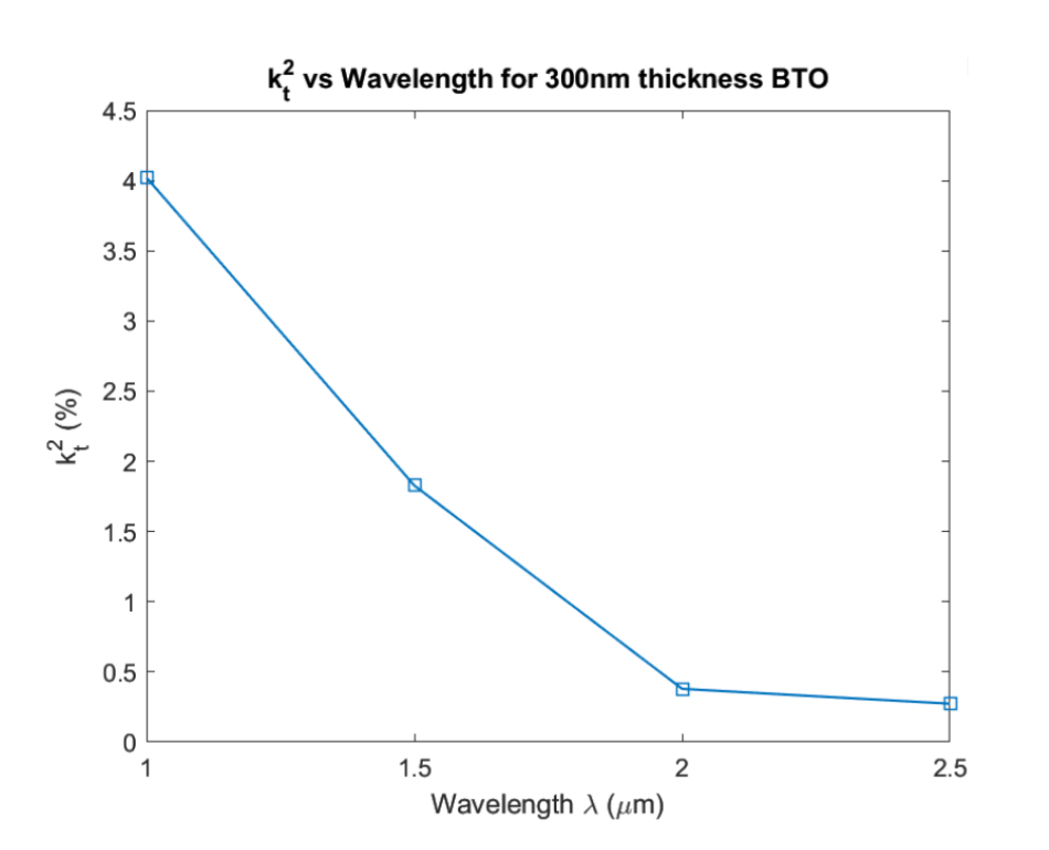
Plot of Coupling Efficiency vs. Wavelength for 300 nm thick BTO excited by a Rayleigh Mode. Although the Sezawa modes showed to have a higher coupling efficiency, the difficulty in containing those waves within the device led to a focus on optimizing BTO excited by Rayleigh acoustic modes.
After manipulating the physical variables shown in Figure 3, further testing was done by changing the number of IDT fingers, adding additional IDT fingers to increase the reflection of SAWs, and varying the thicknesses of these reflection IDT fingers and the aluminum. Figure 10 highlights the parameter space that was the most efficient. Additionally, the scattering parameter S11, which measures input voltage reflection, was used, as seen in Figure 11. Ideally at resonance frequency a small S11 reflection is desired, which indicates that at that frequency the majority of the energy is dissipated as acoustic energy. The optimized parameter space led to new SAW device designs that will be utilized for new device fabrication.

Although 300 nm thick BTO, with its accompanying IDT parameters, was found to have the best efficiency, we also had existing SAW devices on 120 nm thick BTO with specified IDT parameters made by collaborators in Clemson University. Our focus was shifted to simulating with the current device’s IDT parameters to get a sense of what its efficiency and resonance frequency would be, seen below in Figures 11 and 12, in order to actually use the device. However, initial simulation studies and comparison to the optimized IDT designs validated that the current SAW devices being used had suboptimal parameters, indicating a low level of coupling efficiency as well as admittance. In order to verify the findings done by simulation, the fabricated SAW devices had to be tested. To actually use the devices, the BTO of the device had to be poled first using PFM.


In PFM, an AC voltage is applied between the AFM tip and sample surface to generate a piezoelectric field in the sample. The sample will either contract or expand due to this applied voltage resulting in a deflection of the PFM cantilever. This cantilever deflection is monitored with a standard photodiode detector and demodulated with a lock-in amplifier. By applying a DC bias voltage, it is possible to switch the ferroelectric domains of the BTO as seen in Figure 13.

Since the polar axis (the direction of poling) of BTO aligns with the horizontal direction, lateral PFM measurements were also taken. Figure 14 is a close-up image of the BTO next to an aluminum IDT electrode. The dark and bright regions may be indicative of different ferroelectric domains.

Below in Figure 15 is an example of what unpoled BTO appears as during PFM measurements. The unpoled BTO can be identified by the uniform excitation occurring when a voltage is applied. The wider image view also highlights the alternating electrode fingers and BTO.

Based on the images obtained via PFM, it seemed that IDT device parameters were dependent on the parameters of the BTO sample, which affected the poling ability of BTO and PFM imaging. For example, several papers identified that the values of the piezoelectric coefficient d33, the electromechanical coupling factor k, and dielectric constant ε reach a maximum for a grain size of approximately one µm [2,3,4]. Grain size is the individual crystalline areas that form within a material. The structure, size, and orientation of these grains are based on the material composition and method of forging. Since BTO uses sintering, a process of forging that can be relatively well controlled, it follows that extra time and attention is put into fine tuning what are essentially the foundations of the material and consequently its interesting physical properties as a piezoelectric and ferroelectric material.
Conclusion
With this project, optimal parameters for BTO and SAW devices were found through analyzing the process of poling. We found that the poling ability of BTO seems to have a dependence on grain size, temperature, and the polar axis of the material. Since initial results confirm that BTO is capable of being poled, the next step will focus on attempting to pole BTO with more optimized conditions to obtain improved results.
In addition, we learned how to do PFM and AFM and use the data collected by these microscopy methods. With the results gained, we confirmed that PFM is indeed a good tool for studying the degree of poling in a material. In the future, the lab will do the same with new SAW devices and BTO samples.
Through simulation, new IDT designs compatible with current sample parameters, as well as for any future devices made by the lab, were created. One possible aspect to work on in terms of simulation is creating a COMSOL model that encompasses greater variables such as the static electric field of air versus the substrate and PFM cantilever tip. Since thin-film materials are much more susceptible to outside forces, such as the PFM probe and its associated electric field [5], it is possible a more detailed simulation would benefit the lab during the experimental process of attempting to measure a signal.
The information found from this study serves as a small step of progress towards the overall goal of eventually developing a piezo-optomechanical device that can successfully undergo microwave-to-optical quantum transduction and consequently, tremendously expand the potential of superconducting quantum circuits.
Acknowledgements
I would like to thank my PI, Mohammad Mirhosseini, for the amazing research opportunity and mentorship, my co-mentor, Hao Tian, for taking me on as a research assistant, as well as the other members of the Quantum Engineering Lab, for creating a welcoming and supportive environment.
Thank you to the Molecular Materials Research Center and Kavli Nanoscience Institute (KNI) for the use of their facilities, and the KNI SURF-the-WAVE Prize Fellowship and WAVE Fellows program for their gracious funding in making this research possible.
References
[1] Delsing, Per, et al. “The 2019 Surface Acoustic Waves Roadmap.” Journal of Physics D: Applied Physics, vol. 52, no. 35, 2019, p. 353001, https://doi.org/10.1088/1361-6463/ab1b04. Section 2. Quantum acoustics with surface acoustic waves in semiconductors
[2] P. Zheng et al., “Grain-Size Effects on Dielectric and Piezoelectric Properties of Poled BaTiO3 Ceramics,” Acta Materialia 60, no. 13 (August 1, 2012): 5022–30, https://doi.org/10.1016/j.actamat.2012.06.015.
[3] Yu Huan et al., “Grain Size Effect on Piezoelectric and Ferroelectric Properties of BaTiO3 Ceramics,” Journal of the European Ceramic Society 34, no. 5 (May 1, 2014): 1445–48, https://doi.org/10.1016/j.jeurceramsoc.2013.11.030.
[4] Yanli Huang et al., “Grain Size Effects and Structure Origin in High-Performance BaTiO3-Based Piezoceramics with Large Grains,” Journal of the European Ceramic Society 42, no. 6 (June 1, 2022): 2764–71, https://doi.org/10.1016/j.jeurceramsoc.2022.01.026.
[5] J. H. Wang, “Substrate Effects on Piezoresponse Force Microscopy Electromechanical Responses of Piezoelectric Thin Films,” International Journal of Solids and Structures 128 (December 1, 2017): 149–59, https://doi.org/10.1016/j.ijsolstr.2017.08.024.
